Qunfa Silicon Photonics Fabrication (Fab) achieves full-flow manufacturing of Optical Phased Array (OPA) chips using pure silicon photonics processes, overcoming material and structural limitations of traditional technologies. It possesses comprehensive process capabilities including high-precision lithography, low-loss thick-film deposition, dry etching, and optical coupling testing.
As the only enterprise in China with fully integrated capabilities spanning silicon photonics device simulation design, manufacturing, packaging/testing verification, and product sales, the Fab is equipped with a Process Design Kit (PDK) for silicon photonics integrated circuits. It demonstrates complete process development and volume manufacturing readiness for 180nm-node silicon photonics platforms, adaptable for wafer processing requirements across diverse products including optical communications and optical sensing.
Leveraging proprietary high-end silicon photonics chip process solutions, the Fab has established a specialized R&D and process engineering team. It provides complete manufacturing services tailored to customer requirements, delivering a solid foundation for technology transfer and industrial scaling within the silicon photonics sector.
Process
Equipments
Occupied Areas
Core process module
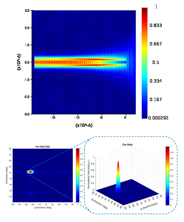
Simulation & Design
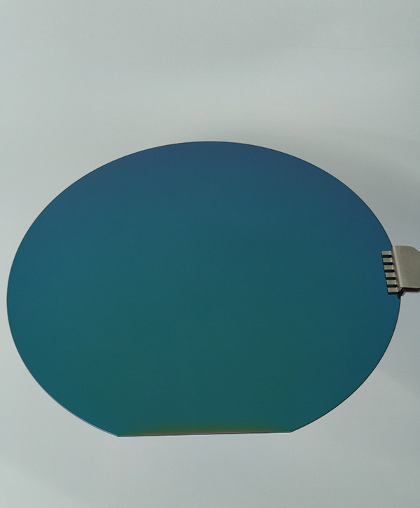
Deposition
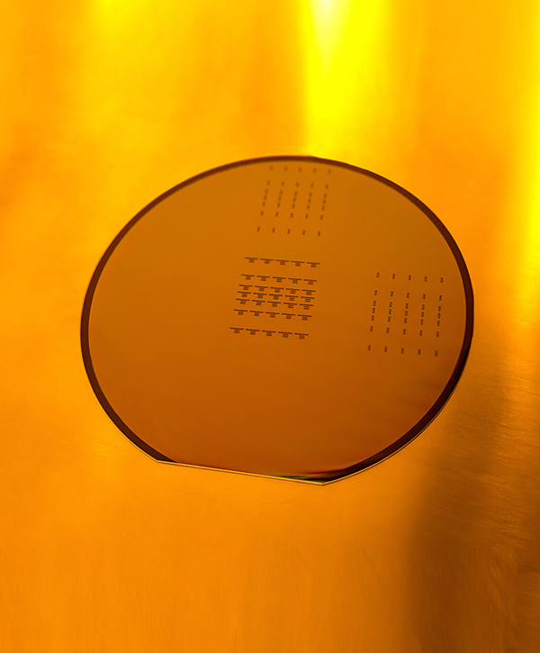
Lithography
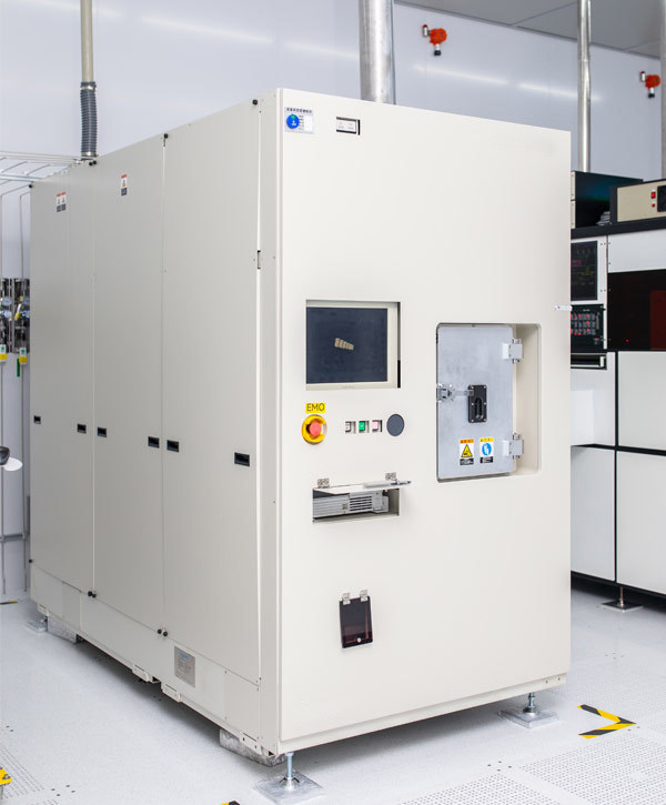
Etching
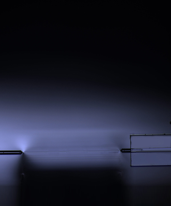
Coupling & Testing
Service process
02
Obtain PDK
Upon receipt of the NDA document signed by the user, the PDK file will be sent to the user's registered email address.
03
Multi-Project Wafer (MPW) Shuttle Service
Please select an appropriate shuttle cycle with reference to the production schedule and submit your reservation to: sales@yzqunfa.cn.
Upon receipt of the reservation documentation, an official order confirmation shall be dispatched to your registered email address within three (3) working days. Kindly monitor your designated inbox for this correspondence.


