Yangzhou Qunfa Photonics Technology Co., Ltd.


Explore our latest updates and industry perspectives
Mass production of OPA silicon optical chips promotes technological breakthroughs in multiple fields
Publish Time:
2025-05-09
According to MEMS Consulting reports, On April 27, The 2025 Yangzhou Silicon Photonics Industry Development and Qunfa Optoelectronics OPA Pilot Line Launch and Product Launch Conference was held in Yangzhou. Industry experts and corporate representatives from the silicon photonics field gathered together to conduct in-depth discussions on the cutting-edge applications of optical phased array (OPA) technology.
In the afternoon exchange activity opening remarks, Professor Yi Yashasha, chief scientist of the collaborative project between Qunfa Optoelectronics and the University of Michigan, delivered a report on 3D Integrated Photonics. Professor Yi mentioned:
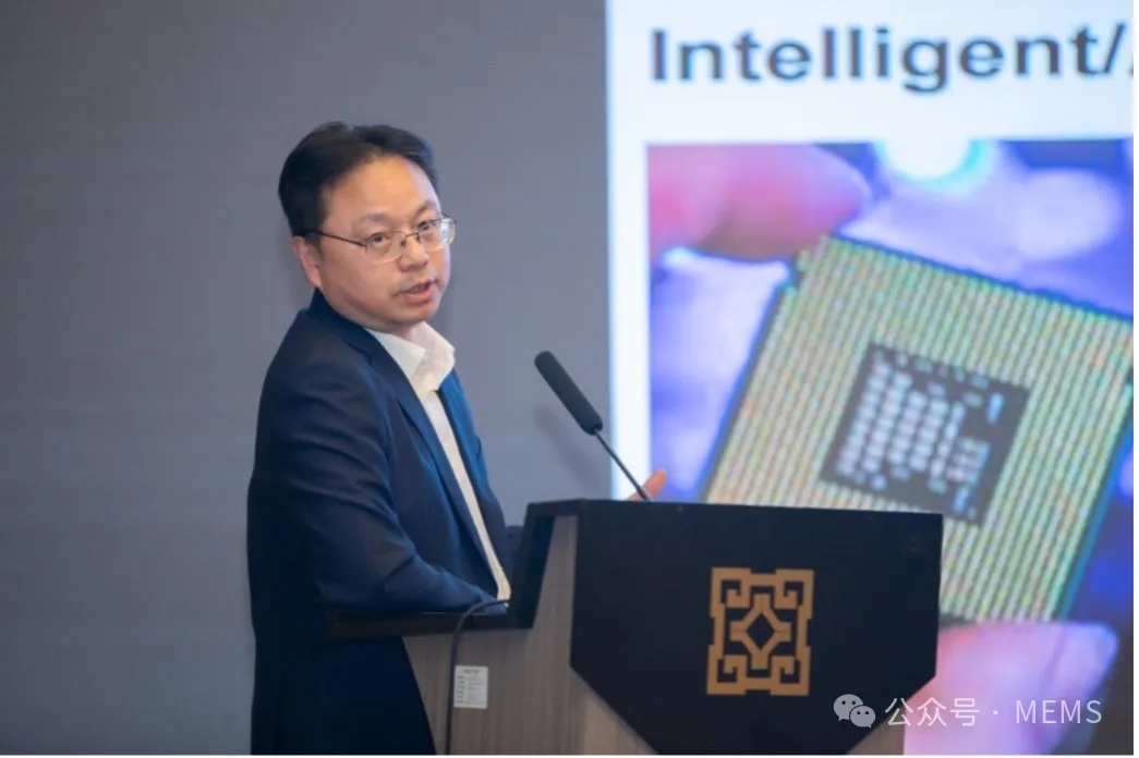
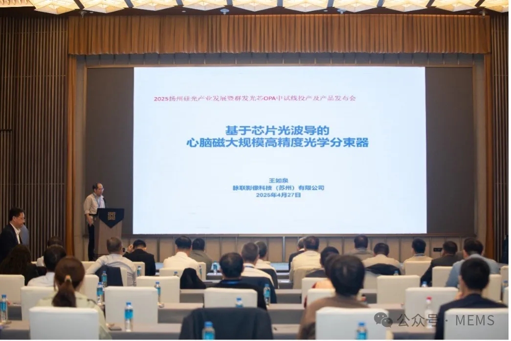
3D integrated photonics is a key path to breaking through the performance bottlenecks of traditional planar optical chips. By achieving vertical bonding of heterogeneous materials (such as InP and Si) on a silicon-based platform, laser, modulator, and detector components can be integrated at high density to construct a "miniature photonic system" on the chip. The completion of Qunfa Optoelectronics' OPA pilot line will be based on low-loss thick-film silicon nitride manufacturing technology, assisting in the processing of various types of silicon photonic devices, gradually building a large-scale 3D integrated optical array system, and laying the foundation for subsequent applications in sensing, medical, and communication fields. Wang Ruquan, Chairman of PulseLink Imaging Technology: "Large-scale high-precision optical beam splitter for heart and brain magnetic fields based on chip optical waveguides"
Dr. Wang Ruquan focused on the detection of weak biomagnetic fields, revealing
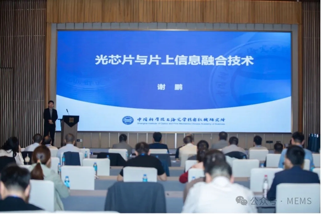
the innovative application of OPA technology in the field of weak biomagnetic field detection. Addressing the pain points of large size and high cost (annual cost exceeding 2.5 million yuan per unit) of superconducting quantum interference device (SQUID) equipment, the OPA solution can achieve a chip-level optical waveguide beam splitter—achieving high-precision beam splitting of 128 optical signals (non-uniformity <0.88 dB), providing a stable light source for the optical pump magnetometer array. Subsequently, wearable brain magnetic helmets (905g) based on this can be verified and tested, which is expected to promote the popularization of applications such as epilepsy localization and autism screening in children, with the cost of a single device expected to be reduced to one-fourth of the original cost. Xie Peng, researcher at the Shanghai Institute of Optics and Fine Mechanics, Chinese Academy of Sciences: "Optical Chips and Parallel Optical Computing Technology"
Researcher Xie Peng discussed the potential of optical chips in the field of parallel optical computing. He mentioned that electronic chips are limited by the von Neumann architecture bottleneck, while optical chips, with their light-speed transmission and parallel processing characteristics, can achieve high-speed computation of massive data. Among them,
silicon photonic chips based on OPA technology can achieve parallel transmission and processing of data through optical phase control, demonstrating advantages over traditional electronic computing in scenarios such as artificial intelligence and cryptography decryption, providing a new path for computing power breakthroughs in the "post-Moore era". Professor Zhan Qiwen, Shanghai University of Technology:
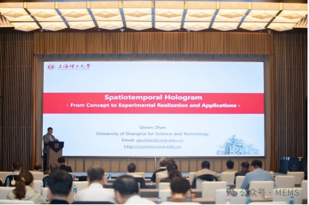
Spatiotemporal Hologram: from Concept to Experimental Realization and Applications Professor Zhan Qiwen of Shanghai University of Technology shared the latest international spatiotemporal holography technology. Spatiotemporal holography uses
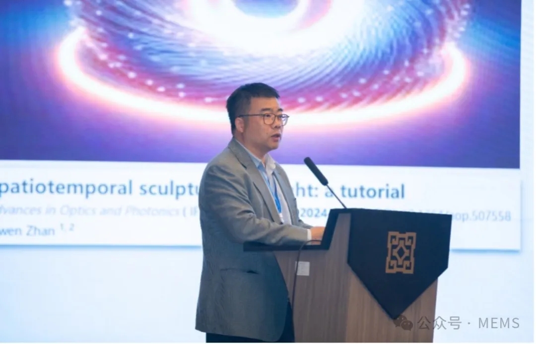
OPA technology to precisely modulate the spatiotemporal dimensions of light, breaking through the static limitations of traditional holography and achieving dynamic three-dimensional holographic display. This technology has disruptive application potential in virtual reality, high-end security, and bioimaging, such as real-time reconstruction of three-dimensional dynamic images of human tissues in the medical field, providing visualization support for precise diagnosis and treatment. Lian Bo, Executive President of Guangdong Semiconductor Industry Association: "Multi-field Applications and Industrialization Panorama of Silicon Photonic Chips"
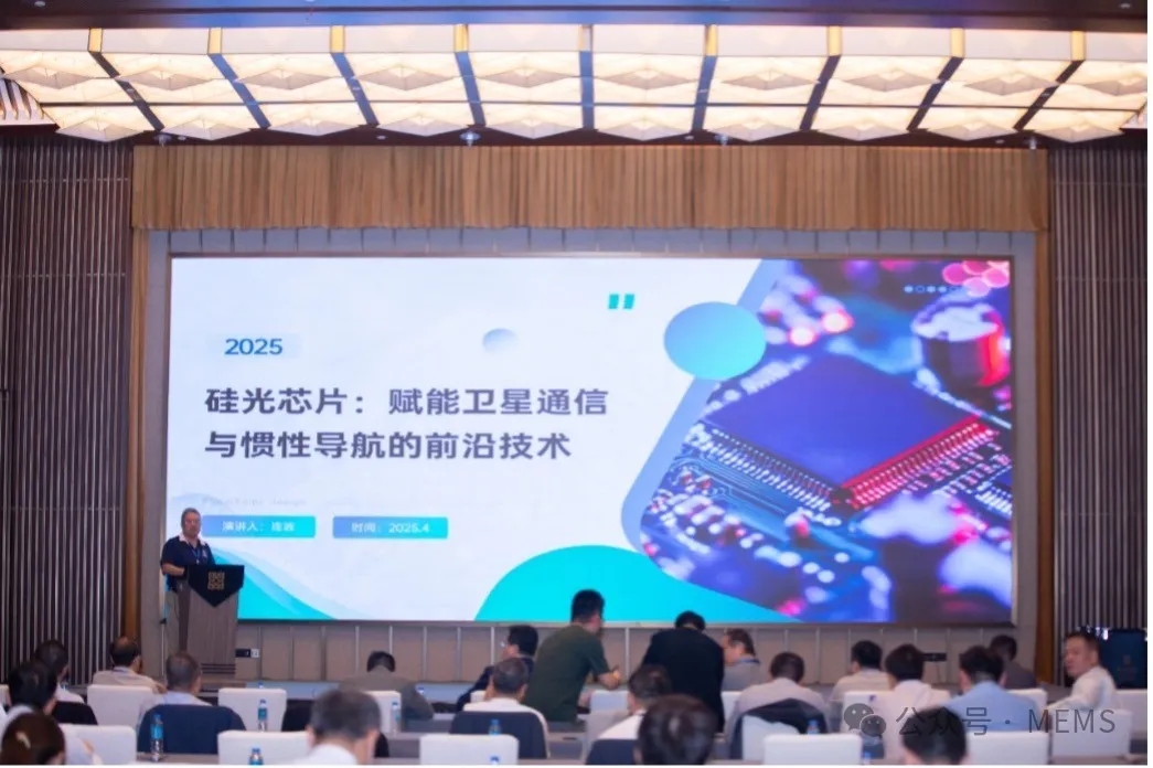
President Lian Bo comprehensively analyzed the landscape of silicon photonic chips in the satellite communication industry. In the aerospace communication field,
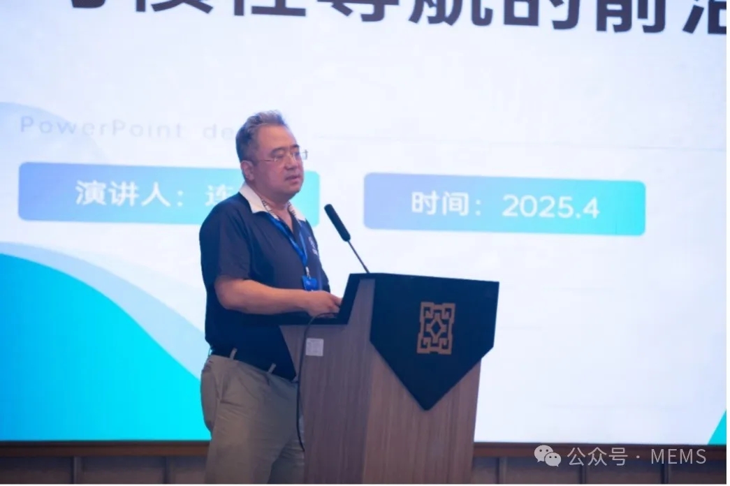
OPA chips, with their excellent cost control and performance requirements, help low-orbit satellites achieve inter-satellite communication exceeding 100 Gbps, with weight and power consumption reduced by 60% and 70% respectively compared to traditional solutions. In inertial navigation, the OPA-based silicon optical gyroscope (SiOG) has a volume compressed to 1 cm³, a start-up time of <1 second, and will push the navigation accuracy of autonomous driving (L4/L5 level) to a new level, with an estimated market size of US$4.6 billion in 2028. Gong Xiang, Chief Scientist of Wuhan Tianmou Optoelectronics: "Application Exploration of Silicon Photonic Chips in LiDAR"
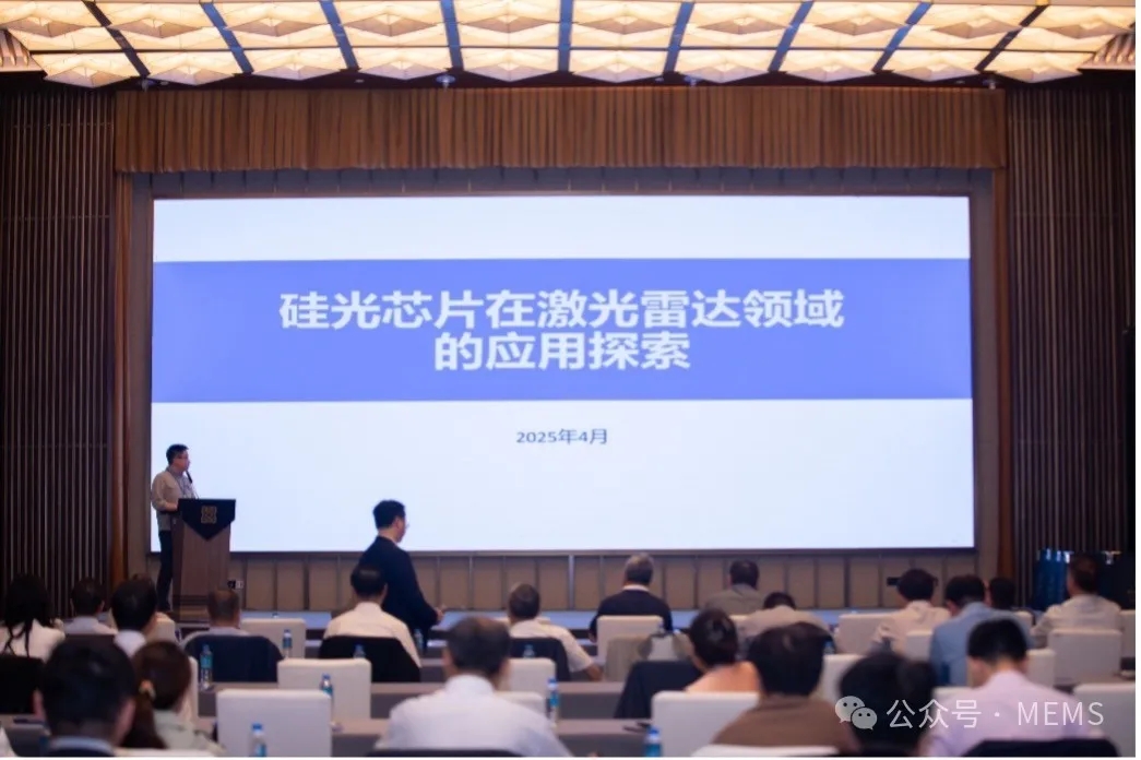
Gong Xiang, chief scientist of Wuhan Tianmou Optoelectronics, focused on intelligent driving and demonstrated
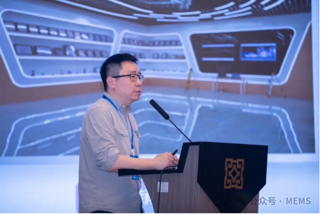
the innovation of OPA technology for the solidification of LiDAR. Traditional mechanical and semi-solid-state LiDARs are limited by volume, lifespan, and reliability, while the OPA+FMCW solution achieves detection distances exceeding 200 meters through silicon photonic chip integration technology, improves anti-interference capability by 30 dB, and reduces the volume to 1/10 of traditional solutions. The mass production of 64-channel OPA chips by Qunfa Optoelectronics' OPA pilot line has pushed the cost of a single LiDAR to the thousand-yuan level. Currently, Tianmou Optoelectronics has reached a strategic cooperation with Qunfa Optoelectronics and is expected to launch an OPA LiDAR prototype solution in the near future. At the afternoon exchange meeting,
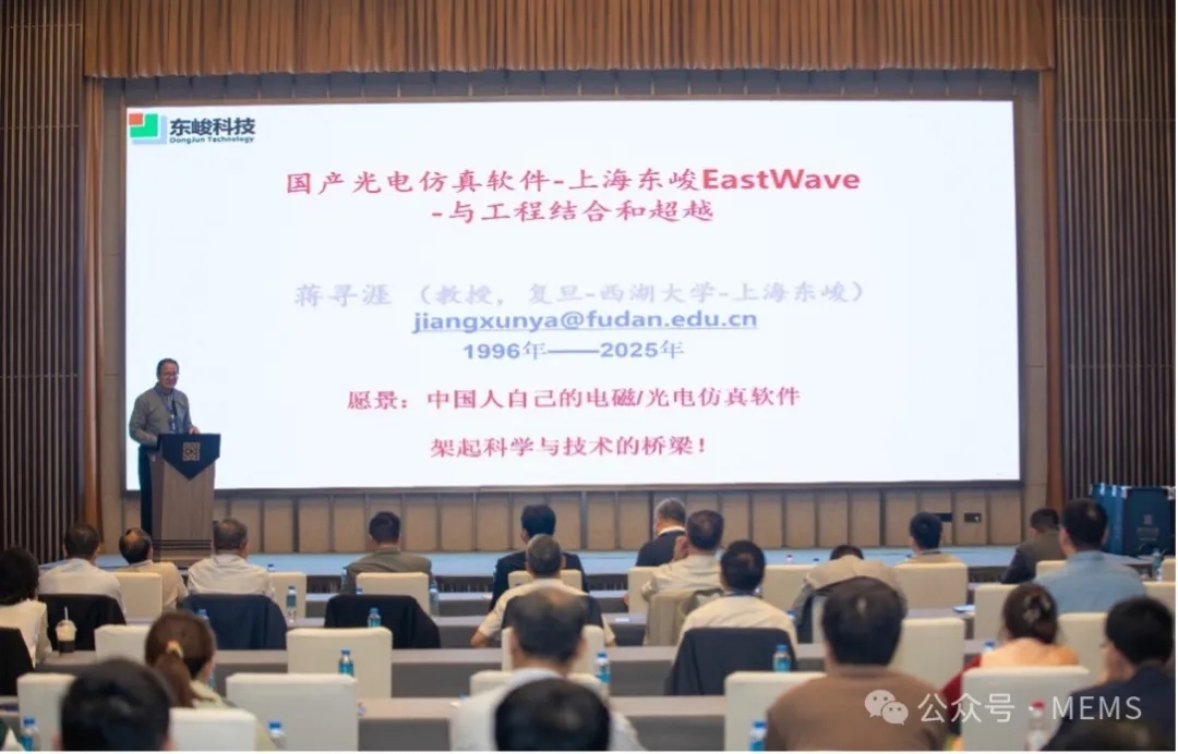
Professor Jiang Xunya from Fudan University introduced the breakthrough path of domestically produced optoelectronic simulation software. For a long time, European and American commercial software has monopolized the optoelectronic simulation field, but the EastWave software developed by Professor Jiang's team has achieved high-precision simulation of optical chips, optical fiber devices, etc., through independent algorithm innovation, and in some complex scenarios, the computing efficiency and accuracy surpass international counterparts. Its latest progress will further empower the domestic silicon photonics industry, reduce R&D costs, and accelerate the transformation speed of cutting-edge integrated optical technologies such as OPA from theoretical design to engineering implementation.
This exchange meeting focuses on the industrial extension of OPA technology, from the bottom-up breakthrough of 3D integrated photonics to the cutting-edge exploration of heart and brain magnetic detection, parallel optical computing, and spatiotemporal holography, and then to the industrial application of communication, navigation, and LiDAR, outlining a panoramic view of the silicon photonics industry driven by OPA technology.
Among the attendees, in addition to the speakers who gave wonderful presentations, there were also experts and scholars and senior practitioners from various fields such as LiDAR, spectrometers, low-altitude economy, MEMS, etc. They exchanged and discussed with the speakers and the Qunfa Optoelectronics technical team on cutting-edge directions such as wind-measuring LiDAR, miniature spectrometers, the precise sensing needs of unmanned aerial vehicle clusters in the low-altitude economy, and the heterogeneous integration trend of CPO packaged optical chips.
Guest interaction and exchange MEMS等多元领域的专家学者和资深从业者。他们分别围绕测风激光雷达、微型光谱仪、低空经济中无人机集群的精准感知需求,以及CPO封装光芯的异构融合趋势等前沿方向与演讲嘉宾和群发光芯技术团队展开交流探讨。

嘉宾互动交流1
嘉宾互动交流2
Mass-produced optical chips The launch of the OPA pilot production line is not only a milestone for the Yangzhou silicon photonics industry, but also marks China's leap towards the center stage in the field of photonic integration. Starting with OPA technology, Qunfa Optical Chip has been deeply cultivating 3D optical phased array chips and silicon photonic integration technology, while continuously expanding its boundaries into strategic fields such as intelligent sensing and satellite communication. Through cross-industry collisions, it showcases the diverse application potential of OPA technology and provides excellent Qunfa optical chip solutions for future technological integration and scenario innovation.
Contact Us

WeChat Official Account
Copyright © Yangzhou Qunfa Integrated Photonics Technology Co. Ltd.